Introduction
Our research group is affiliated with the Laboratory of Silicon-Based Materials and Integrated Devices at the Shanghai Institute of Microsystem and Information Technology, Chinese Academy of Sciences. We are dedicated to advanced research in the field of integrated circuit materials, focusing on the study and innovation of silicon-on-insulator (SOI) materials and devices, 300mm silicon wafer planarization, aluminum nitride (AlN) materials and devices, electron beam sources, electronic chemicals, material analysis and characterization, and materials genomics, etc.
Our group emphasizes interdisciplinary collaboration and industry-academia-research synergy. Achievements include: the original proposal and successful development of embedded cavity silicon-on-insulator (VE-SOI) materials and devices; the industrialization of key technologies for 300mm silicon wafer planarization; the invention and development of a 200mm full-wafer high-throughput thin-film deposition and characterization PVD-ALD-XPS cluster equipment; the establishment of a materials genomics technology system for integrated circuits; the world-leading performance of ultra-high-frequency AlN RF devices; and the development of a prototype electron beam source based on porous silicon.
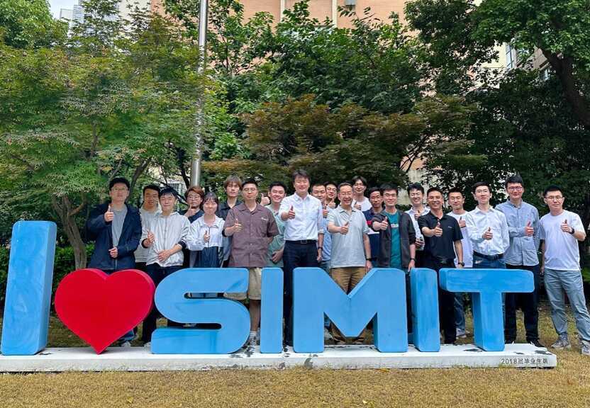
We possess a comprehensive platform for the characterization and analysis of integrated circuit materials, a synthesis and preparation platform, and an applied R&D platform. The current team consists of 32 members, including 3 senior researchers, 5 associate senior researchers, 2 junior and intermediate researcher, 3 project managers, 5 postdoctoral fellows, and 14 doctoral and master's students. Among them are 1 national leading talent in scientific and technological innovation, 1 high-level talent introduced by Shanghai, and 2 recipients of the Chinese Academy of Sciences' Hundred Talents Program.